Breakthrough in domestically produced EUV lithography machines? Good news for Huawei chips! US semiconductor embargo rendered useless?
the day China feels comfortable sharing news about its EUV progress will not only be a momentous breakthrough in the chip semiconductor sector, but also a moment of collective brilliance for Chinese assets on the global stage.
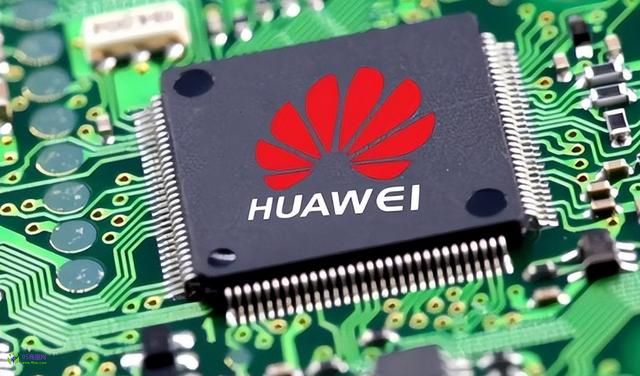
In the past two days, there have been numerous reports about domestic substitutes for Huawei-related chips, including the latest progress in EUV lithography machines, advanced packaging technologies, and the large-scale procurement of computing power centers.ShenTeng910C chips, etc. These reports have attracted widespread attention, but which ones are truly reliable and which are just unverified essays? This article will sort out these reports in detail and explore their potential impact on the semiconductor sector.
EUV lithography: Cautious optimism on good news
Among all the domestic alternatives, the progress of the lithography machine is undoubtedly the most concerning.Recently, there have been reports from self-media that Huawei's Dongguan base is installing and testing domestic EUV lithography machines,and has already entered the trial production process.However, it is important to note that this information has not been officially confirmed at this time.

From the details of the news, it emphasizes a breakthrough in the light source, namely the laser-induced plasma technology (LDP) of Harbin Institute of Technology. It is not news that China has chosen a completely different path from ASML LPP technology in the production of EUV light sources.
Although LDP technology has the advantage of higher light source efficiency, it also has its disadvantages. When ASML tried this technology path in the past, it was abandoned due to poor stability. However, the latest news does not mention whether China has solved the stability problem of this technology, so the authenticity of this news needs to be verified as a whole.
Indeed, news about domestic EUV lithography machines has never ceased this year.
We know that,the light source, objective lens, and double workbench are the three major core components of the photolithography machine. In March of this year, there were reports that the photolithography objective lens had entered the commissioning phase.

Combining this information, two things are beginning to emerge:oneis that there is not just one team within the country working on EUV lithography, one possibility is Shanghai Micro Electronics, the other is a force led by Huawei-related companies;twois that although there is no official confirmation of a breakthrough in EUV lithography at present,it is certain that our country is making efforts to move forward. We are currently promoting it in a low-key manner, and the reasons are well understood by everyone.
We should maintain cautious optimism about the progress of the photolithography machine. The advancement of technology cannot be accelerated merely by passion; we look forward to good news that we can achieve overtaking on the curve based on respecting the laws of science.
Advanced packaging: making up for shortcomings to break through difficulties
Although the news of EUV photolithography machines is yet to be further confirmed, there is actual progress in the field of advanced packaging of domestic computing power chips —— Huawei's four-chip packaging patent exposed. The patent aims to encapsulate four computing power chips and 16 HBM (High Bandwidth Memory) chips together.

As early as the beginning of June,Huawei's president Ren Zhengfei mentioned in a media interview that China's chips are restricted by equipment, and the single-piece performance of our chips lags behind that of American chips, but we can break the deadlock by stacking or clustering, with the ultimate goal of making artificial intelligence computing performance comparable to that of American chips.
Currently, Huawei's mainstream productShen Teng910B, its single-piece performance compared to Nvidia's H100,is about only 30% to 40%.Through this four-chip packaging technology, multiple 910B chips are packaged together to form a super chip with performance basically comparable to H100.
This patent was applied for as early as April last year, and it was only recently made public,so the market has been speculating that the technology might be used to produce Huawei'sAscend next-generation product 910D.

It is worth mentioning that NVIDIA's advanced packaging of chips requires EUV lithography machines to support, becauseit needs to drill holes on the silicon wafer; while Huawei's advanced packaging technology does not require drilling holes, ingeniously avoiding the restrictions of EUV equipment, while also achieving extremely high transmission efficiency. This precisely confirms what Mr. Ren said, "Use mathematics to make up for physics, and use non-Moore to make up for Moore".
Computing chips: Steady increase in volume shows strength
Besides advanced packaging, another definite good news is related to Ascend 910C.The 910C is actually two 910B packaged together, and its yield is low because of the lack of advanced equipment in our country, which once worried about whether its capacity could keep up.
However, on June 6th, a 10,000-level hub computing center in Xinjiang released a tender notice, explicitly stating the purchase of 4,500 910C servers. This move indicates that the 910C is being produced in increasing quantities.

Combining the advanced packaging technology mentioned above, we can clearly feel that,our country is steadily moving forward on the road of high-performance computing chips with independent control, each step is solid and powerful.
This is not only the inevitable choice for China's technological rise, but also a fierce breakthrough under external pressure.Even if we did not choose this difficult path on our own, the US's occasional technological blockades and restrictions would always remind us of the urgency and importance of achieving technological independence and control.
US sanctions:搬 stones to kick the foot to promote self-improvement
Just in the last couple of days, the US Department of Commerce released a message saying that it is very likelyto cancel the exemption for foreign companies in China for US-made equipment in theirfabs.This development can be traced back to the Biden administration, when the US enacted new export control regulations in 2022 aimed at preventing Chinese companies from obtaining semiconductor production equipment with US technology.
But at the time, exemptions were granted to companies like South Korea, Japan and Taiwan that had factories in mainland China. Now the US is threatening to rescind that exemption.

In fact, what really matters is not Chinese companies, but the United States and its allies. For the US allies, what they are worried about is whether their own businesses can continue to operate, such as Samsung, which has a large capacity in mainland China; while US companies are more worried that such restrictions will provide strong ideological motivation for China's self-reliant development path.
Predictably,the day China feels comfortable sharing news about its EUV progress will not only be a momentous breakthrough in the chip semiconductor sector, but also a moment of collective brilliance for Chinese assets on the global stage.
In summary, we see both hope and challenges in the process of domestic替代 of Huawei's chips. For unverified information, we should maintain rationality and caution; while for the actual progress that has been made, we should give full affirmation and expectation.
It is believed that in the near future, with the continuous breakthrough of technology and the continuous development of the industry, China's semiconductor industry will surely usher in a more brilliant tomorrow.
Permalink: http://www.chinaservicesnet.com/article/73.html(Reprint with permission)
